


Blog
PCB Assembly Lead Time: Prototype to Volume, Explained

PCB assembly lead time is the schedule from file review to shipped, tested boards. It is not a fixed number – it depends on component availability, board complexity and the test steps you require. Understanding the stages helps you set a realistic delivery date.
The stages of an assembly schedule
- File review and quotation: engineering checks the Gerber, BOM and CPL and confirms scope
- Component sourcing: availability check and ordering of long-lead or at-risk parts
- PCB fabrication: bare boards are fabricated while components are ordered
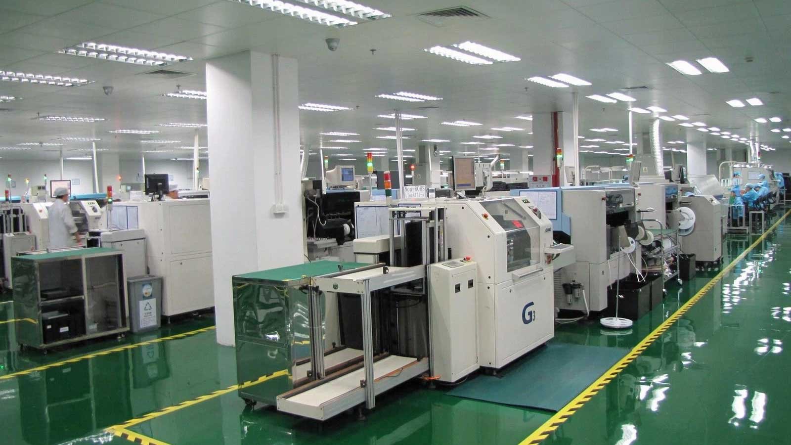
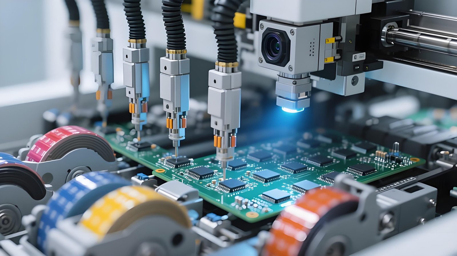
- Assembly: solder paste, placement, reflow, and through-hole work
- Inspection and testing: AOI, X-ray and functional testing per the quality plan
- Packing and delivery: final QA and shipment records
What typically slows a project down
- Incomplete or changing BOM data
- Long-lead or obsolete components
- New tooling such as ICT fixtures
- Late file changes after the build is released
Planning around component availability is the single biggest lever. KGPCBA confirms a project-specific schedule covering fabrication, SMT assembly and testing during the file review, so the delivery date is part of the quotation rather than an afterthought.