


Blog
SMT Assembly Process Explained: From Stencil to Reflow

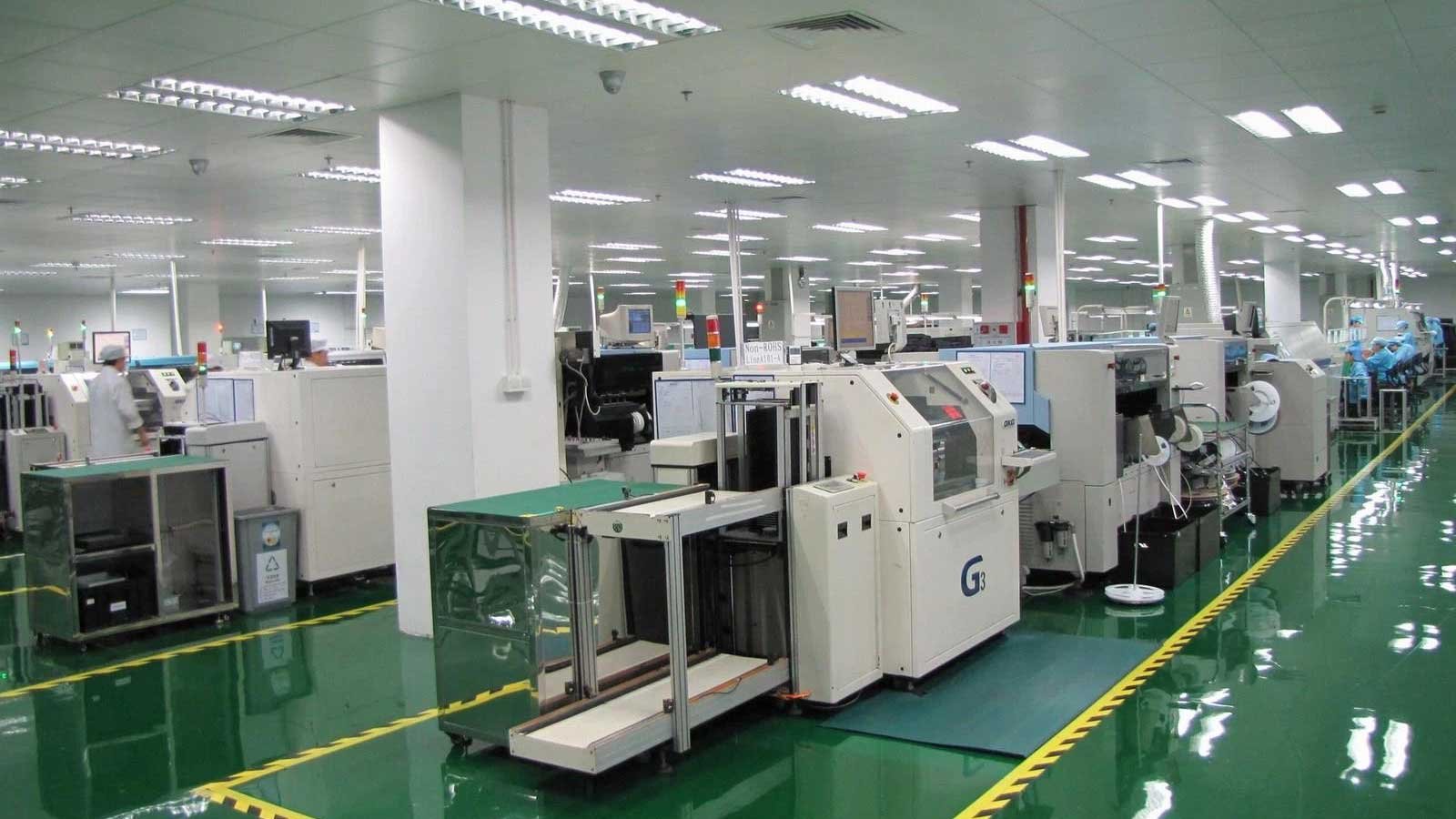
Surface-mount technology (SMT) is how the vast majority of modern electronics are assembled. Understanding the process helps you design for manufacturability and read assembly reports with confidence.
Step 1: Solder paste printing
A stainless-steel stencil is aligned to the board, and solder paste is printed onto the pads. The stencil aperture design and paste quality set the foundation for every joint on the board.
Step 2: Component placement
Pick-and-place machines position each component from reels and trays according to the CPL/XY data. Placement accuracy is critical for fine-pitch packages like QFP and BGA.
Step 3: Reflow soldering
The board passes through a reflow oven with a controlled temperature profile: preheat, soak, reflow and cooling. The profile is tuned to the board mass and component mix so paste melts and joints form without damage.
Step 4: Inspection and test
Automated optical inspection (AOI) checks placement and solder joints in line. X-ray verifies hidden BGA and QFN joints, and functional testing confirms the board works.
Designing for SMT means keeping a consistent pad layout, clear fiducials and panelization that suits the line. KGPCBA reviews your files for the SMT process before quoting, with inspection and testing selected per project.
3 thoughts on “SMT Assembly Process Explained: From Stencil to Reflow”